
Vision
Since the last decades, the beam intensity and brilliance of modern particle accelerators and synchrotron light sources have continuously increased. Classical solid-state detector systems are facing serious problems under these experimental conditions. Novel room-temperature qualified sensors are required, which provide extreme radiation hardness and ultra fast response to the impinging radiation. Moreover, for low-background integration of the devices, the nuclear charge of the sensor materials has to be low and the detectors thicknesses have to be minimized.
Advanced CVD-diamond detectors are promising replacements or complements of traditional devices, for instance, of silicon-diode sensors or plastic scintillation counters. In unique manner, diamond combines all the required physical properties described above. It is especially expected that single-crystal CVD-diamond sensors will be superior in the following important detector categories:
- Particle tracking near the interaction points of colliding nuclei.
- In-beam start detectors of time-of-flight measurements.
- Beam/Beam-loss monitoring of intense, focused particle or X-ray beams.
Project and Objectives
The focus of our work is the development of large-area radiation-hard CVD-diamond detectors of high granularity and spatial resolution. Aiming at the reduction of the total material budget along the particle tracks, new detector designs and readout techniques will be investigated in addition. The project comprises three main R&D lines:
- The development of 2D sensors consisting of large, freestanding Diamond-On-Iridium (DOI plates).
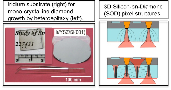
- The investigation of 3D diamond sensors using three types of detector-grade CVD-diamond: homoepitaxial single-crystal CVD diamond (scCVDD) grown on small diamond substrates; polycrystalline CVD diamond (pcCVDD) grown on large silicon wafers, and heteroepitaxial single-crystal diamond grown on wafer-scale iridium substrates (DOI).
- The development of monolithic diamond pixel detectors. The basic structures here are produced by laser-enhanced bonding of diamond sensors on their silicon readout electronic chips. They are named Silicon-on-Diamond (SOD) devices.
Until now, two types of CVD-diamond detectors have been established within the particle physics community. The large pcCVDD sensors of reduced charge-collection efficiency but of excellent time resolution and count-rate capability and the small scCVDD samples showing both good time and energy resolution [1]. Meanwhile all over the world these sensor types are implemented in a variety of physics experiments and beam diagnostic applications at accelerator infrastructures.
However, so far it was not possible to combine highest diamond quality with large sample areas. This fact prevented, for instance, the application of single-crystal diamond for particle tracking at LHC and other high-energy facilities. Larger ‘quasi single-crystal’ diamond plates can be produced by heteroepitaxy on iridium substrates, in particular, on the multilayer structure Ir /YSZ/ Si001. Iridium provides the best matching set of physical parameters for highly oriented diamond growth [2]. Iridium substrates as large as 4 inch in diameter are routinely produced at the University of Augsburg - one of the worldwide leading institutions in the engineering of detector-grade DOI layers. The upcoming task will be the extension of the homogeneous diamond nucleation layer over the whole area of the substrates.
In the framework of the HGF Detector Platform, the detector properties of intrinsic DOI plates produced in Augsburg will be characterized with different methods at the participating institutions. Novel detector designs and readout techniques will be investigated in conjunction with commercial and new-developed readout electronics for diamond sensors [3]. At CEA-LIST Saclay and the University of Manchester, the development of 3D diamond sensors on scCVDD plates already showed excellent progress, while at the INFN in Florence, the first monolithic SOD probes are also delivering encouraging results [4].
Task Allocation
| CEA/UM | 3D diamond detectors - manufacture and tests. |
| DESY | Electrical characterization of DOI and other sensors. |
| GSI | Electrical characterization of DOI and monolithic pixel sensors. Development of front-end electronics and novel readout technologies for high resolution position-sensitive diamond detectors of low material budget. |
| HIJ | Beam tests of diamond detector prototypes. |
| INFN | Manufacture of SOD structures and SOD detector prototypes. |
| KIT | Irradiations. Investigation and evaluation of the radiation hardness of diamond sensor prototypes. |
| UA | Engineering of iridium substrates and DOI films. Studying chemical and structural defects of the DOI samples by application of a multitude of solid-state physics characterization tools. |
Milestones
| 2013 | Production, characterization and tests:
|
| 2014 |
|

